In a multi-disciplinary approach FIXIT addresses the challenge to develop an innovative ultra-low power ferroelectric computing platform. Thereby, FIXIT encompasses all aspects starting from the development of ferroelectric materials and corresponding manufacturing process technologies via ferroelectric device design starting at TRL1, characterization, modeling and hybrid integration or packaging together with conventional CMOS designs towards the demonstration of seamlessly embedded integration into electronic systems. Our final goal is the demonstration of superior energy efficiency and performance of our computing platform in an AI-driven sensing-application at TRL4.
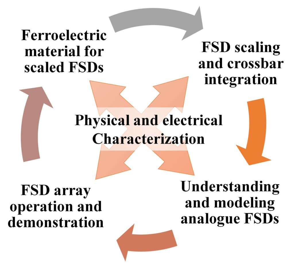

Within FIXIT we will investigate selected 2- and 3-terminal high-impedance ferro-synaptic device (FSD) concepts. All these devices have in common that their operation relies on the tuning of their high-impedance behaviour by modulating the polarization of a ferroelectric layer. Ultra-low read and write currents make these device concepts suitable as resistive switching devices for application in passive crossbar array architectures, that is, without the need for integration of additional selector devices.
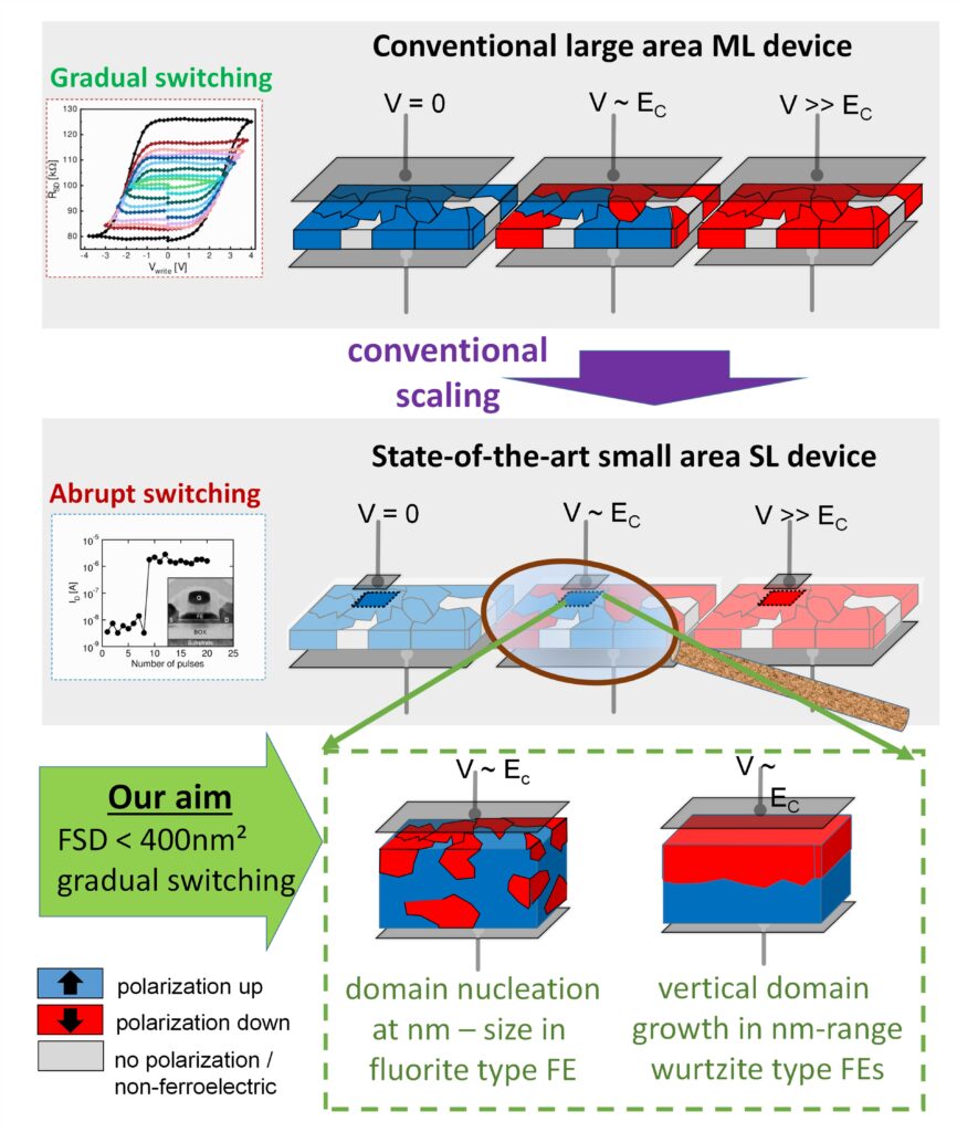
The scalability of ferroelectric synaptic devices (FSDs) is ultimately governed by the underlying properties of the ferroelectric material. Whether their storage capabilities appear analog or not is tied to the number of individual polarization states in the device and the material. Solutions available today for analog switching typically require active areas > 104 nm² up to several µm². This is due to the still relatively large grain and domain size in available ferroelectric thin films. However, this drastically limits the energy efficiency and device density of state-of-the-art FSDs. Through advanced material engineering, FIXIT aims to reduce the footprint required for FSDs by close to two orders of magnitude – down to ≤ 20 nm x 20 nm.